
Voltera V-One
The Voltera V-One is a PCB Prototyping system from voltera.io. And we just got one having put in a pre-order in April 2017. So we made the default “Hello World”project to make sure it works. And it did. Now the first serious assignment is making a single sided PCB with eight channels of third order active low pass filtering on it. Although it can do double sided PCBs there are extra steps so I started with single sided and we will run a few jumper wires to stitch the GND and VCC nets together. Everything else I was able to route fully through on the top layer. You can watch it in action below.
And this is the design it is printing. Below is the schematic for 2 of the low pass active filter channels.
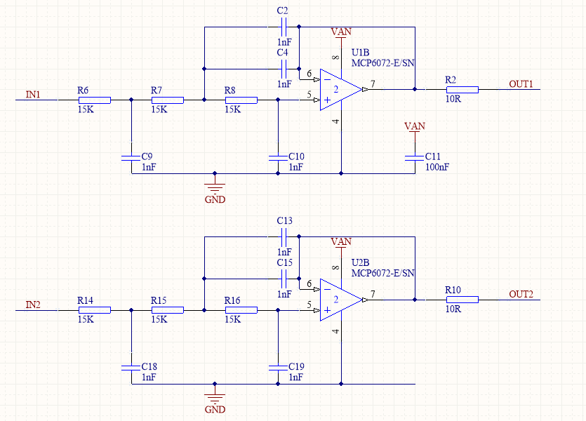
Active Low Pass Filter Schematic
The layout that was then converted to Gerber plots (only needed the GTL top layer) and printed. You can easily see where I allowed for the jumper wires. The ones on the left are GND and on the right are VCC.
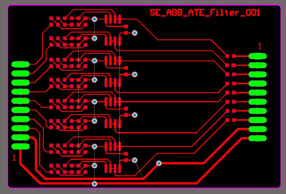
Active Low Pass Filter PCB
This technology is the equivalent of 3D printing for circuit boards. But wait, there is more. You can use any substrate so this can print on glass or a flexible medium such as Kapton. And it is worth noting that it is a printer and so can handle more than just conductive ink. You can also use it as a general purpose printer. It will even dispense paste on standard HASL finish production PCBs so you can do stencil free reflow of standard PCBs.
They are also working on a milling attachment and we plan on getting that as soon as it is available.
Voltera V-One Review
Here is a review put together by Andrew Walla. I’ve added a few comments of my own so here it is.
Voltera V-One Pros
- Voltera have done an exceptional job with the software user interface and look and feel of the product. In much the same way that the Arduino platform makes embedded micro-controller technology accessible to the masses, I feel the V-One does the same for PCB prototyping.
- The printer has everything you need to get started to print your own “Hello World” project. Batteries are included.
- The printer allows you to fabricate single layer PCBs in less than a day, even on unusual substrates such as glass or flexible polymers.
- Double sided PCBs are supported. There are extra steps such as drilling the through holes after curing the first side then aligning the second side then print and cure. A simple double sided PCB could also be done the same day. You manually fill Via holes with paste so they plate through.
- The printer accepts standard PCB file formats (GERBER) and doesn’t appear to have any difficulty reading them correctly.
- The printer allows for aligning different designs over pre-existing prints or for double sided PCBs.
- It also has a paste dispenser so you can lay down paste and then hand load components.
- The heated bed, used for curing the conductive ink, will go hot enough to reflow the paste once you have parts loaded. You can even modify the temperature profile to behave in a custom manner.
- If you have standard PCBs with HASL finish then they have a specific paste you can use with them and it will reflow those as well. We are likely to make a lot of use of that feature. And the machine is faster at this than printing because the ink curing time is an hour but paste is ready to go the moment it is dispensed.
- The conductive ink seems to live up to its promised conductivity.
- And the biggest Pro of all: if you need a PCB today, then you can have your PCB today, as long as it is within the process capabilities of the Voltera V-One.
So lots of positives there.
Voltera V-One Cons
- Don’t expect this printer to make production quality PCBs for you.
- It doesn’t support solder masks. Plus that would take up a lot of ink. So you will want to think about whether you want to coat the PCB after assembly with a varnish.
- And there is a lot more work to getting a double sided board together.
- You also won’t end up with as neat a result as you can get from production PCBs hand loaded. However the paste dispenser is definitely going to get a lot of use on HASL finish PCBs so we see that as a major win.
- Because the PCB sits on top of the rails when it is being cured, you can’t run tracks out to the edge of the PCB.
- We made some cardboard spacers to allow us to position the blank PCB in the centre of the bed. Otherwise it can be awkward to get the printing aligned with the PCB. So this is an area that needs improving.
- And while they do intend to release a milling accessory, it isn’t ready yet. That is also on our “to get” list.
Overall, I have been quite impressed and look forward to seeing what this printer will have to offer in future.
This post was jointly produced by Ray Keefe and Andrew Walla.
Successful Endeavours specialise in Electronics Design and Embedded Software Development, focusing on products that are intended to be Made In Australia. Ray Keefe has developed market leading electronics products in Australia for more than 30 years. This post is Copyright © 2017 Successful Endeavours Pty Ltd.