

Printed Electronics
Way back in 2011 we looked at the state of Printed Electronics and concluded this was a rapidly emerging area of Technology and had been since the previous look at The Future of Low Cost Electronics Manufacture in 2009. It has been a while so what has happened since then?
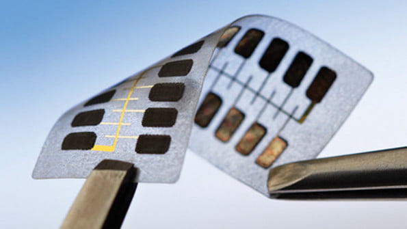
Printed Electronics
This is another guest post by Andrew Walla.

Andrew Walla
Printed Electronics Overview
Rapid prototyping, also referred to as 3D printing or additive manufacturing is the process of building objects or devices by building up layer by layer [1]. It has been identified as a potentially disruptive technology in the manufacturing industry in the coming years and is particularly well suited to provide benefits to technologies that operate on smaller scales of production [2]. New manufacturing paradigms, such as direct manufacturing (directly printing the sold goods) and home manufacturing (providing the capability for consumers to produce parts themselves) are set to change the way that small manufacturing businesses operate and significantly increase the level of competition in the industry [3].
This post will discuss the manufacturing technique of printing – a technology whose origins date back more than five centuries [4] and in this time a number of different printing methods have been developed. Successive layers are generally printed onto a substrate either by direct contact; via an impression cylinder (such as in flexographic, graviture or offset printing), deposited via a stencil (screen printing); or directly deposited onto the substrate (for example, inkjet printing, aerosol-jet printing or organic vapor-jet printing). Of these technologies, inkjet printing is particularly well suited to rapid prototyping and low volume manufacturing due to its high customisability, relatively high resolution and relatively low set-up cost [1].
Inkjet printed electronics differs to conventional inkjet printing in that the deposited substances need to exhibit desired electronic behaviours. A common method to achieve this is to intersperse the ink (a solvent) with nano-particles (small particles with controlled sizes, typically in the order of nano-meters) with desired conductive, dielectric or semiconducting characteristics. The printed substance might be treated post printing in order to evaporate the solvent and/or facilitate a chemical change in the nano-particles. Examples of such treatment include thermal curing [5], curing by ultraviolet light [6], laser sintering [7], e-beam sintering [8], chemical sintering [9] or plasma sintering [10].
Current research efforts are focusing on improving the printing and post-processing technologies available [10-12], improved interconnects [13] and vias [14], improved semiconductors, and printing under less stringent conditions. Examples include printing conductors at room temperature [6] and printing elements such as transistors [15] and diodes [16] with ever increasing performance characteristics. It is forecast that these improvements will continue for some time, as the fastest known inkjet printed transistor has an operating speed of around 20MHz [17-18]. (This is several orders of magnitude behind the capability of existing silicon chip technology.) Researchers are also working on developing transistor characteristics other than maximum frequency. For example, inkjet printing technology has been used to produce flexible and transparent transistors [19].
For those looking to predict where printed electronics will have the greatest future impact, it may pay to think outside the box. In the author’s opinion, inkjet printing technology is likely to play a larger role in enabling new applications than it is to replace existing electronic technology. It is unlikely that a device with the functionality of a smartphone will be printed any time soon, but perhaps the capability of printing your own solar panels is closer than you think.
[1] N. Saengchairat, T. Tran and C.-K. Chua, “A review: additive manufacturing for active electronic components,” Virtual and Physical Prototyping, vol. 12, no. 1, pp. 31-46, 2017.
[2] A. O. Laplume, B. Petersen and J. M. Pearce, “Global value chains from a 3D printing perspective,” Journal of International Business Studies, vol. 47, pp. 595-609, 2016.
[3] T. Rayna and L. Striukova, “From rapid prototyping to home fabrication: How 3D printing is changing business model innovation,€” Technological Forecasting & Social Change, vol. 102, pp. 214-224, 2016.
[4] S. H. Steinberg, Five hundred years of printing, Maryland: Courier Dover Publications, 2017.
[5] N. Graddage, T.-Y. Chu, H. Ding, C. Py, A. Dadvand and Y. Tao, “Inkjet printed thin and uniform dielectrics for capacitors and organic thin film transistors enabled by the coffee ring effect,” Organic Electronics, vol. 29, pp. 114-119, 2016.
[6] G. McKerricher, M. Vaseem and A. Shamim, “Fully inkjet-printed microwave passive electronics,” Microsystems & Nanoengineering, vol. 3, p. 16075, 2017.
[7] S. H. Ko, H. Pan, C. P. Grigoropoulos, C. K. Luscombe, J. M. J. Fréchet and D. Poulikakos, “All-inkjet-printed flexible electronics fabrication on a polymer substrate by low-temperature high-resolution selective laser sintering of metal nanoparticles,” Nanotechnology, vol. 18, pp. 1-8, 2007.
[8] Y. Farraj, M. Bielmann and S. Magdassi, “Inkjet printing and rapid ebeam sintering enable formation of highly conductive patterns in roll to roll process,” The Royal Society of Chemistry, vol. 7, pp. 15463-15467, 2017.
[9] S. Wunscher, R. Abbel, J. Perelaer and U. S. Schubert, “Progress of alternative sintering approaches of inkjet-printed metal inks and their application for manufacturing of flexible electronic devices,” Journal of Materials Chemistry C, pp. 10232-10261, 2014.
[10] Y.-T. Kwon, Y.-I. Lee, S. Kin, K.-J. Lee and Y.-H. Choa, “Full densification of inkjet-printed copper conductive tracks on a flexible substrate utilizing a hydrogen plasma sintering,” Applied Surface Science, vol. 396, pp. 1239-1244, 2017.
[11] J.-J. Chen, G.-Q. Lin, Y. Wang, E. Sowade, R. R. Baumann and Z.-S. Feng, “Fabrication of conductive copper patterns using reactive inkjet printing followed by two-step electroless plating,€” Applied Surface Science, vol. 396, pp. 202-207, 2017.
[12] H. Ning, R. Tao, Z. Fang, W. Cai, J. Chen, Y. Zhou, Z. Zhu, Z. Zeng, R. Yao, M. Xu, L. Wang, L. Lan and J. Peng, “Direct patterning of silver electrodes with 2.4 lm channel length,€” Journal of Colloid and Interface Science, vol. 487, pp. 68-72, 2017.
[13] T. Ye, L. Jun, L. Kun, W. Hu, C. Ping, D. Ya-Hui, C. Zheng, L. Yun-Fei, W. Hao-Ran and D. Yu, “Inkjet-printed Ag grid combined with Ag nanowires to form a transparent hybrid electrode for organic electronics,” Organic Electronics, vol. 41, pp. 179-185, 2017.
[14] T.-H. Yang, Z.-L. Guo, Y.-M. Fu, Y.-T. Cheng, Y.-F. Song and P.-W. Wu, “low temperature inkjet printing and filling process for low resistive silver TSV fabrication in a SU-8 substrate,” 30th IEEE International conference in Micro Electro Mechanical Systems (MEMS), 2017.
[15] J. Roh, H. Kim, M. Park, J. Kwak and C. Lee, “Improved electron injection in all-solution-processed n-type organic field-effect transistors with an inkjet-printed ZnO electron injection layer,” Applied Surface Science, vol. 420, pp. 100-104, 2017.
[16] K. Y. Mitra, C. Sternkiker, C. Martinez-Domingo, E. Sowade, E. Ramon, J. Carrabina, H. L. Comes and R. R. Baumann, “Inkjet printed metal insulator semiconductors (MIS) diodes for organic and flexible electronic application,” Flexible and Printed Electronics, vol. 2, no. 1, p. 015003, 2017.
[17] X. Guo, Y. Xu, S. Ogier, T. N. Ng, M. Caironi, A. Perinot, L. Li, J. Zhao, W. Tang, R. A. Sporea, A. Nejim, J. Carrabina, P. Cain and F. Yan, “Current Status and Opportunities of Organic Thin-Film Transistor Technologies,” IEEE Transactions on Electron Devices, vol. 54, no. 5, pp. 1906-1921, 2017.
[18] A. Perinot, P. Kshisagar, M. A. Malfindi, P. P. Pompa, R. Fiammengo and M. Caironi, “Direct-written polymer field-effect transistors operating at 20MHz,” Scientific Reports, vol. 6, pp. 1-9, 2016.
[19] L. Basirico, P. Cosseddu, B. Fraboni and A. Bonfiglio, “Inkjet printing of transparent, flexible, organic transistors,” Thin Solid Films, vol. 520, pp. 1291-1294, 2011.
Andrew Walla, RF Engineer
So there has been some substantial change but we aren’t yet at the point where this type of Electronics Design and Manufacture has begun to significantly disrupt the mainstream industry. But I can imagine the day when some of what I do now can be printed and tested right now on my desk instead of having to go through PCB Design, PCB Manufacture and Electronics Prototyping first. Can’t wait for Printed Electronics to become mainstream.
Successful Endeavours specialise in Electronics Design and Embedded Software Development, focusing on products that are intended to be Made In Australia. Ray Keefe has developed market leading electronics products in Australia for more than 30 years. This post is Copyright © 2017 Successful Endeavours Pty Ltd.