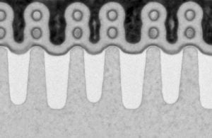
FinFETs Rule
At the moment, the dominant transistor technology used to make high density silicon devices is the FinFET. This is made using vertical fins allowing the gate to wrap around the Source and Drain. This improves control of the channel.
Some additional details are available at FinFET
FinFETs have dominated dense semiconductor design and manufacture since 2011 and are the reason we have been able to continue driving device density higher while not increasing heat by the same amount.
Beyond FinFETs
So what comes next?
It is believed the logical next step is to fully wrap the gate around the source and drain region creating a Gate-all-around Device. This gives maximum control while also reducing leakage to transistors either side. Nanotechnology researcher imec has demonstrated one method of achieving this by wrapping a silicon gate around 8nm wide nanowires. This Lateral Nanowire Gate All Around FET could prove to be a candidate to replace FinFETs as the demand for device density continues to grow.
And an isometric view of the Lateral Nanowires and the gate structure wrapped around them.
One benefit of this approach is that the fabrication process is very similar to FinFET fabrication and so the transition to the new technology might not require significant investment in new equipment. This is quite different to shrinking the technology from 10nm to 7nm or 5nm which usually required significant research, process development and equipment reinvestment.
Interesting times ahead.
Successful Endeavours specialise in Electronics Design and Embedded Software Development, focusing on products that are intended to be Made In Australia. Ray Keefe has developed market leading electronics products in Australia for more than 30 years. This post is Copyright © 2016 Successful Endeavours Pty Ltd.


