
Printed Circuit Board Assembly
Also referred to as a PCA, the Printed Circuit Board Assembly follows on from Printed Circuit Board Manufacture. This is where the components are placed onto the PCB or Printed Circuit Board and the electrical connections formed.
In this post I will focus on volume manufacturing techniques. We also make Printed Circuit Board Assemblies in house by hand loading very small quantities. This is appropriate for prototypes and Niche Manufacturing quantities.
To start with, let’s look at the two types of components we most work with. The first type is the Through Hole Component. These have pins that go through the PCB to make electrical connection. These components dominated PCB Assemblies until the 1980s when higher PCB loading density requires a change of technology. They are still widely used where mechanical strength, tall components, heavy components or high current levels are involved. An example is shown below with the connectors, relays, transformers and removable components as Through Hole with the Surface Mount Components toward the centre:

Through Hole Technology
The second type is the Surface Mount Component or Surface Mount Device and the overall process is referred to as Surface Mount Technology or SMT. These devices do not require holes through the PCB to mount them and so can be placed closer together and it also improves track routing options because tracks can run on the other side of the PCB without having to avoid the through holes. An example of all Surface Mount assembly is shown below in close up:

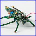
Electronics Hardware
Printed Circuit Board Assembly Process
The infographic below was provided by Algen Cruz of Advanced Assembly in the USA. Algen also provided a brief explanation to go with it and I have added that as well. You can click on the infographic to view a larger version.

Printed Circuit Board Assembly
“Design-for-Assembly (DFA), although not as well known as Design-for Manufacturing (DFM), needs to be taken into account during the design phase. And the first step in being able to design-for-assembly is to understand the assembly process. This infographic features this process by showing how a board goes from an unpopulated printed circuit board (PCB) to a final product, ready to be packaged and sent to consumers.” Algan Cruz
Successful Endeavours specialise in Electronics Design and Embedded Software Development. Ray Keefe has developed market leading electronics products in Australia for nearly 30 years. This post is Copyright © 2015 Successful Endeavours Pty Ltd.