PCB Layout
After the Schematic Capture component of the Electronics Design is complete, the logical connections for the electronics components have been determined. If the Electronics CAD package also supports it, you can add rules to guide the Printed Circuit Board Layout, also abbreviated to PCB Layout which we will use from here on.
The PCB provides both the mechanical support for the components and is many cases is a critical part of the circuit since the length of tracks, their thickness, their clearance from other tracks and the relative placement of components and tracks can significantly influence the final performance of the PCB. This is particularly true as power levels, clock speeds or frequency increases.
The Electronic Schematic defines the electrical connections between components, the value of components such as resistors, capacitors and inductors, the type of semiconductors used (silicon chips) and the connectors that take signals and power on and off the PCB. Each item on the schematic has to be linked to a physical shape that will go onto the PCB. This is done by assigning a footprint to the schematic item.
Schematic Symbol
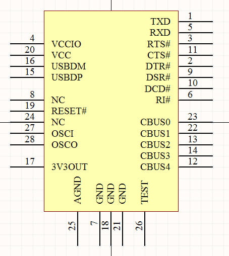
I will explain it works. The Schematic Symbol for an FT232RL USB Serial Interface device is shown below. This is arranged with the signals conveniently placed to suit logical connections and to make the overall Schematic easy to read and understand. The signal name is shown inside the symbol boundary, and the pin number of the IC package is shown on the outside.
FT232RL Schematic Symbol
Schematic Circuit
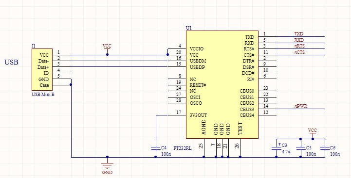
So this is the symbol for a single part, an IC or Integrated Circuit. The Schematic Circuit or Electronic Schematic shows the connections to the other parts of the circuit. Below we see USB connector wired up the the FT232RL IC and the power supply bypass capacitors. The logic level UART signals are shown at the top right. This section of the Electronic Schematic provides the logical connections for a USB serial interface.
PCB Footprint
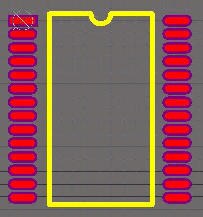
Before we can do the PCB Layout, we have to associate the PCB Footprint each Schematic Symbol will use. The PCB Footprint for the FT232RL IC is shown below.
This is one of the 2 possible footprints for the FT232RL. This one is a 28 pin SSOP package.
Once each Schematic Symbol has a PCB Footprint, we are ready to do the PCB Placement.
PCB Placement
The first step is to create the outline for the PCB and its mounting points, then to place each PCB Footprint so it is in the correct place. For some components, such as connectors, there is a specific place it must go. For other components, there is more freedom to choose the position and there are groups of components that must be in a specific relationship to each other. An example of this are the power supply bypass capacitors which must go very near to the IC they are supporting.
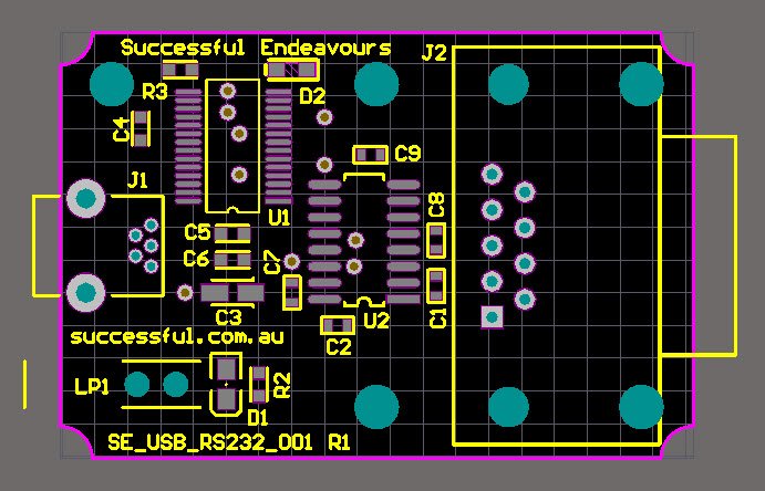
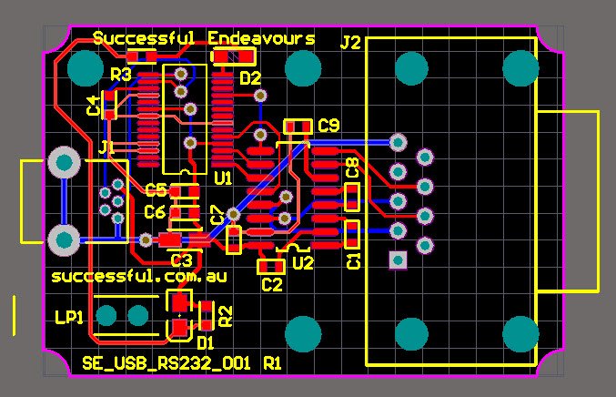
An example of a completed PCB Placement is shown below. This is a USB to RS232 serial converter.
PCB Routing
Now we have the components where we want them, we turn on the auto-router and the PCB is finished. Sorry but I couldn’t help that. The auto-routing features of most PCB Layout CAD software packages are never as good as doing it yourself. They can be useful for testing the ease of routing for a particular placement. There are a lot of manufacturing considerations that need to be taken into account and track size requirements, either for current carrying or voltage drop, can be hard to define from just the schematic. And example of this is the main system voltage such as VCC. In some parts of the circuit the required current is low so smaller track sizes are OK, whereas other areas need heavier tracks. It isn’t easy to define this at the schematic level because they are all the same signal or Net.
The PCB with the routing complete is shown below. The selection of track size is related to the current the circuit needs to carry. A good reference for determining the track size is provided by the standard IPC-2222A.
PCB 3D Cad Integration
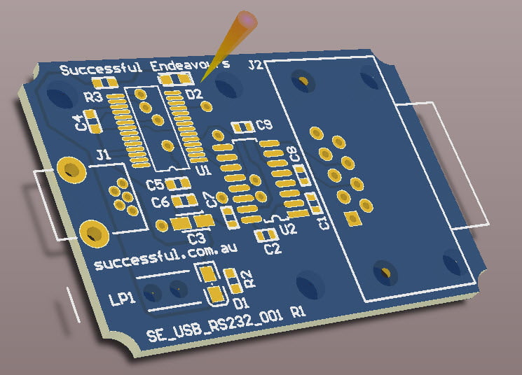
It is also important to make sure the PCB will fit into a mechanical enclosure. Most modern PCB CAD tools, such as Altium Designer which we use, can create full 3D models of the PCB. Shown below is an example of just the PCB without the components showing.
So there we have it. A PCB taken from the completed Electronic Schematic through to a PCB Layout.
Next we will look at prototyping our new PCB.
Successful Endeavours specialise in Electronics Design and Embedded Software Development. Ray Keefe has developed market leading electronics products in Australia for nearly 30 years. This post is Copyright © 2015 Successful Endeavours Pty Ltd.


